Research Activities in the DfX Lab


Design-for-Trust
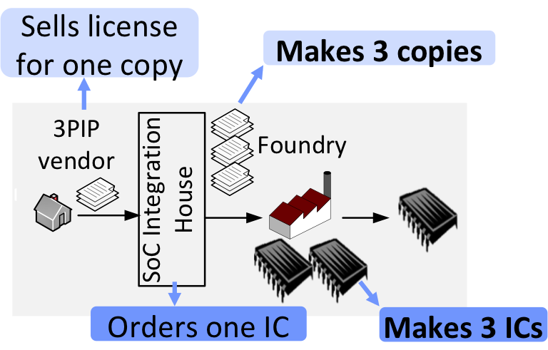
Divide and conquer approach has been proven to be essential in designing multi-billion transistor designs; instead of designing the entire chip from scratch, different parts of the chip are designed by different design teams from different companies, possibly residing in different countries. Fabrication, packaging and testing of these chips are all typically outsourced in offshore locations. Obviously, such a design and manufacturing flow is quite vulnerable to a variety of security threats:
- Hardware trojans: Circuitry implanted into the chips to serve a certain malicious purpose; e.g., freezing the system or allowing a backdoor access to the intruders to leak secret information off the chip.
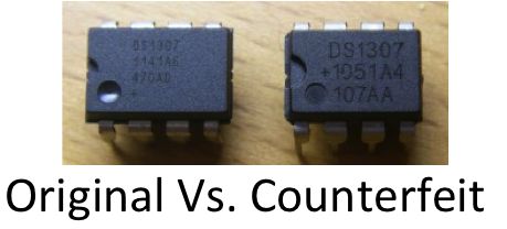
- Counterfeiting: The entry of re-used (old) or cloned chips into the supply chain, resulting in a loss of $100B annually.
- Reverse engineering and IP Piracy: Depackaging a chip, and delayering it to use image processing tools for recovering the design details from the chip layout.
- Side-channel attacks: Analysis of side channels (power, timing behavior) or misuse of on-chip test infrastructure to leak secret information stored on the chip.
We have developed patented solutions to thwart these attacks. Our solutions are:
- Secure logic locking (versions: output corruption based, interference based, SARLock): Additional logic elements (digital lock) are added to the design. Only when the correct secret key is loaded on-chip, these logic elements ensure correction operations on-chip. Otherwise, they break the functionality of the chip.
- Secure IC camouflaging (versions: output corruption based, interference based, CamoPerturb): Cells that look alike under a microscope but can implement one of many possible functions are used in the layout. A reverse engineer is thus puzzled upon encountering these camouflaged cells.
- Secure split manufacturing: Layout is split into two parts (BEOL metal layers and FEOL metal layers), which are fabricated in two different fabs. No single fab has access to complete design information.
- Design-for-Secure-Testability: Scan architecture is minimally tweaked to ensure that information that can be used to infer the secret key will not leak.
- Dynamic Power Analysis (DPA) resilient cipher design

Design-for-Testability
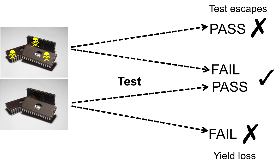
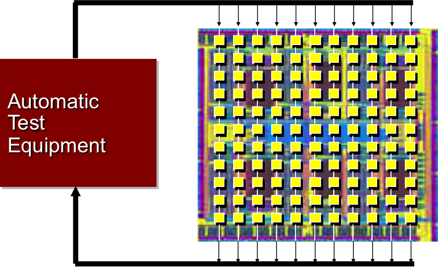
Every single manufactured chip must be tested for manufacturing defects, and today, it is reported that 30% of the overall production cost is due to testing. DfT techniques consist of the design of on-chip hardware blocks along with accompanying software CAD tools that enable the high-quality and cost-effective test of manufactured chips for manufacturing defects. They aim at reducing test costs, while targeting the detection of as many defective chips as possible, ensuring high test quality. DfT techniques in general may incur area, performance and power penalty; the techniques that we propose aim at minimal hit in these aspects while delivering the benefits expected from DfT.
We have developed patented solutions to enable low-cost high-quality test:
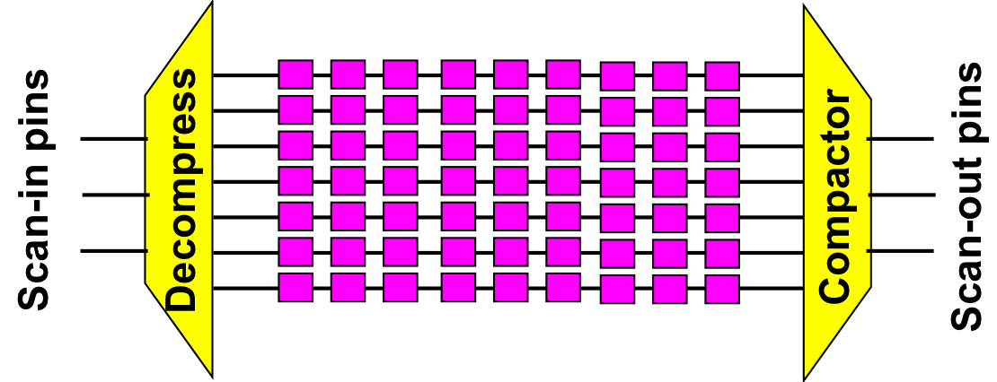
- OCD Architecture: This test architecture enables ultimate control over test pattern encodability, response observability and switching activity. Test time, data volume and power can all be minimized. <3 issued patents>
- Expedited-Compact: Compacting responses on the chip can be performed in a power-frugal manner through employing this technique. Scan-out power can thus be reduced significantly. <pending patent>
- Toggle-based masking: Unknown response bits can be efficiently masked, especially when they are clustered. This technique eradicates unknown response bits by using minimal control information. <issued patent>
- Low-power at-speed testing: Divide and conquer test approach can be enabled through rewind/restore support on-chip. This way launch-off-capture and launch-off-shift test techniques can be conducted with minimal power consumption. <1 issued and 1 pending patent>
