Design-for-Trust Techniques
IC Camouflaging
Many commercial ICs such as TI 4377401 baseband processor, and Intel’s 22nm Xeon processor have been reported to be successfully reverse engineered. Commercial as well as open-source tools for reverse engineering are available. Although reverse engineering has been primarily devised for verifying commercial piracy and patent infringements, it can also be misused by an attacker for stealing the IP.
IC camouflaging is a layout-level technique that hampers imaging-based reverse engineering; this technology was developed by Syphermedia. Camouflaging introduces cells that look alike from the top view but can implement one of many possible Boolean functions. On reverse engineering a camouflaged IC, an attacker cannot infer the correct functionality of the camouflaged cells by inspecting the layout through imaging techniques. IC camouflaging is performed by inserting dummy contacts, filler cells, programmable standard cells, or a combination thereof.
An example camouflaged circuit with two camo gates is illustrated. Each camo gate can implement either a NAND, NOR or XOR; due to the use of dummy contacts, the functionality cannot be inferred from the layout pictures. In the illustration the red gates denotes the actual functionality of the camo gates; the attacker has 9 combinations to try!
The camo gates are bigger, slower and more power-hungry compared to their standard counterparts. Therefore, only a small subset of the gates can be turned into camo gates for practical implementations.


A real and a dummy contact.

The original and the camouflaged circuits. Each camouflaged gate can implement one of three functionalities, unknown to the reverse engineer.
In the example to the right, the camo gates implement either NAND or NOR. To reveal their functionality, the inputs to the camo gate need to be justified to a 10 or a 01, and its output should be sensitized to an output. In the example, a single input pattern do this for both camo gates. The computed pattern 10011 is called an attack pattern.
A working chip can then be used as oracle. The attack pattern(s) can be applied to the chip, and the chip’s response can be used to infer the camo gate functionalities.
As a countermeasure against this attack, we developed a clique-based selection (CBS) of camouflaged gates. A clique is a complete subgraph in a graph. CBS camouflages a set of gates such that the output of a camouflaged gate in the set cannot be sensitized to a primary output of the design without accounting for the other camouflaged gates in that set; this set of camouflaged gates is referred to as a clique. For more information, refer to our papers c74 and c75, or patent p16.


Protecting the minterms is a useful feature in the following scenarios:
- Controllers usually implement one-hot encoding on their activation signals. Hiding the minterm that signals the activation of a particular state can enable IP protection. Without identifying this state, the resultant finite state machine (FSM) will be different from that of the original FSM.
- Access control mechanisms, such as password checkers, enable “valid” signals only for the correct password, in other words, a particular combination of inputs (i.e., minterm). Thus, one needs to protect those circuits from reverse engineering.
- Interrupt controllers initiate interrupts based on a certain combination of processor states, in other words, a particular combination of signals feeding the interrupt controller.
- Most hardware-security modules that help software security techniques use a “go/no-go” signal, “yes/no” signal, or “error/no-error” signal to indicate a safe execution. Examples of such modules include Dynamic Trusted Platform Module, Secure Return Address Stack, and TrustNet and Datawatch. Protecting the minterm that activates these signals can help hide their checking mechanism, making them difficult to bypass.
- There are certain bits in a design, referred to as Architecturally Correct Execution (ACE) bits, whose correctness must be ensured for overall correct operation. Applying logic perturbation on the ACE bits ensures that an incorrect circuit operation will be obtained by a reverse engineering attacker.

The transformed design, when successfully reverse engineered, is minimally different than the original design; they differ in their outputs corresponding to the perturbed minterm only, and are identical, otherwise. In other words, the truth tables are different in a single entry. An attacker needs to identify the secret perturbed minterm to fully reverse engineer the design IP. For that, the attacker is forced to reverse engineer and recover CamoFix.
While the attacker can use a functional chip as an oracle, the simulated model will always minimally mismatch the oracle (one entry in the original truth table). Any attack on camouflaging (e.g., DeCamo) will have to go through a tremendous computational effort to identify this minimal difference (i.e., perturbed minterm); the number of minterms is exponential in the number of inputs. This will also reflect into a number of DIs that is exponential in the number of inputs; due to the way CamoFix is designed, the number of DIs is exponential in the number of camouflaged gates as well.
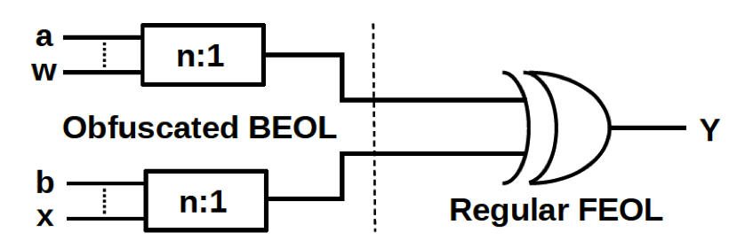
Here we propose a novel camouflaging scheme which is low-cost, resilient, and generic. Our scheme is based on obfuscating the interconnects (BEOL); it can be readily applied to any design without modifications in the device layer (FEOL). Illustrated below are the secret n:1 mapping in the BEOL, which obfuscate the inputs for any regular gate (not only two-input XOR). The set of possible functionalities depends on n:1, the selection of the input nets, and the gate type.